Dual Active Bridge
hardwarepower-electronicsfirmware
Why Dual Active Bridge?
For this project, I wanted to deliver 3kW bi-directionally from 400V and 48V. This used for the Ulysses autonomous charging system. For the actual system, the design is different (so I’m not breaking any NDA’s), but I used this design flow as a reference.
The Dual Active Bridge is an industry standard topology for this kind of voltage conversion at this power level. More recently, it’s become an industry standard in data center server rack power supplies, supplying low voltage to GPU clusters from a high voltage bus. There are a number of topologies that can do the voltage conversion at high power (Resonant LLC, Phase-Shifted Full Bridge, CLLC, etc..). But not many can do bi-directional conversion.
The Dual Active Bridge has two full-bridges synchronously switching, operating off 8 PWM control signals, hence the name Dual Active Bridge. In between the bridges, a transformer performs the stepdown. A series inductance across the primary or secondary winding of the transformer acts as the step-down element, much like other buck-derived topologies.
A phase shift between the first set of PWM (controlling the first full bridge) and the second set of PWM (controlling the second full bridge) controls both the direction of transfer and the magnitude of power transferred.
Planar Transformer
A traditional transformer is N sets of coils wrapped around a transformer core, with the ratio of the primary and secondary determining the voltage conversion. Traditional transformers are tall, bulky, and expensive. Oftentimes, power converters have custom transformers wound for them, which become extremely expensive (often the most expensive part of the converter).
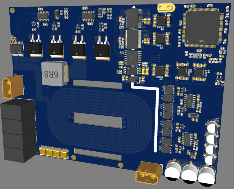
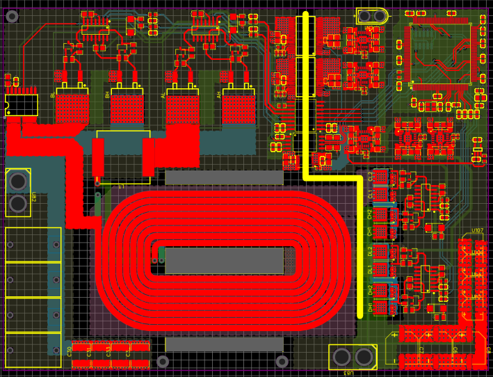
A planar transformer is a transformer that uses trace windings etched into the PCB, often with an E-shaped core that gets embedded into the PCB. In essence, it’s a transformer that’s baked into the PCB, no external windings needed. This has many advantages, including better vertical packaging, controlled leakage inductance, and especially BOM cost, sourcing, and manufacturing. The tradeoff is poorer thermals, a larger planar profile, and a complicated winding structure.
For this project, I wanted to create a maximally flat dual active bridge with a large cooling surface, which can be cooled much more effectively, and which has a better vertical profile.
To tune the leakage inductance of the transformer, I intentionally went with a stack-up that reduced the field coupling, so that I could achieve a higher leakage inductance. However, this ended up not mattering much in the end, because the resulting leakage inductance was still too small to not necessitate an external inductor.
The thickness of the traces are a big problem in planar transformers, with the winding requirements and thickness requirements driving up the size of the ferrite cores being embedded into the PCB. I ended up choosing a medium sized core and sacrificing thermal performance for packaging benefits.
Bridging
Gate drives tend be extremely similar no matter what topology, especially for non-isolated designs. You have a half bridge gate drive, with a series external capacitor and diode for bootstrap operation (some gate drivers have internal diodes, but usually never internal capacitors). These drive a half-bridge MOSFET configuration through series resistance, pulldown resistors, etc. The switching node between the top and bottom MOSFETs acts as the floating GND reference for the top MOSFET, so any gate drive components referencing the top MOSFET should be connected to the switching node acting as GND. On the PCB, the switching node should be as small as possible. The power loop for the gate should be as small as possible, with a short path back to the gate drive to minimize the loop inductance. The half-bridges should be laid out as symmetrically as possible. Components for the gate drive chip should be placed as close to the chip as possible, but the gate resistors in the switching path do not need to be placed so close.
For the low voltage bridge on the Dual Active Bridge, there is a maximum of 62A going through, which requires more careful consideration. Usually for high-current bridges, even if an individual MOSFET is rated for 60A on paper, it’s never actually practical to use a single FET for 60A. It is a common practice to parallelize multiple MOSFETs per bridge to decrease the load going through each individual MOSFET. To get a good ballpark of what kind of parallel configuration can handle a given load, it is good to look at reference designs. I ended with two MOSFETs on each parallel branch, each rated to 40A.
Firmware and Controls
For the controls, I am using an STM32H7 series chip, which comes with advanced hardware timers TIM1 and TIM8, and 16-bit ADC’s sampling far faster than the nyquist frequency for this design. Each timer comes with full-bridge PWM driving, programmable dead time insertion, and can be chained together with an internal hardware trigger. A hidden bonus is that the H7 series has a a lot of nice documentation.
Getting CCCV operation requires a double-layered control loop, with voltage and current readings on both the primary and secondary. The control algorithm for both are relatively straightforward, a PI controller does the job. For fully bi-directional operation, the firmware needs to track which side is an input and which is an output, which requires voltage sensing at the input of the high and low voltage busses.
For the precise power control, we follow:
where is power in watts, is the driving frequency in Hz, is the turns ratio, and are the input and output voltages in volts, is the leakage inductance from the transformer (in this case, there is also a series inductance that contributes to this), and is the normalized phase shift ratio between the first and second full bridge control signals.
For extremely low leakage inductance, the phase shift between and has to be extremely small, too small for the firmware to implement. The inductance therefore has to be tuned to match the controls (and the controls have to be tuned to match the hardware).
Things learned from testing
Lots of thermal things here. The primary bridge (high voltage) performed worse thermally than I expected, and the secondary bridge (low voltage) performed better. The windings performed surprisingly well considering they were spec’d undersized, and I expected a higher temperature rise (this means you can get away with even smaller traces). Meanwhile, the series inductor got really hot! It makes sense, but I didn’t account for it while designing.
Positioning Power in the Datacenter World
I’m done talking about my design, this part’s for the broader discussion of power in datacenters. I mentioned earlier that datacenters use DAB and DAB-derived topologies to perform voltage step-downs. As server racks move to higher voltage and as the power demand increases, efficient power conversion becomes ever more important. I’m especially intrigued by the effect that datacenter demand has had on power converter research. Over the last few years, a lot of progress has been made on efficient power conversion, one of the downstream effects of AI. I’m curious to see what advances happen next.